ASML and Moore’s law
February 18, 2025

Electronic circuits have made the increase of computing power an inescapable drum to contemporary life. New computers and phones come out in 18 month-cycles; and at the cusp of each new cycle, electronics seem to be slowing down, cosmically faltering. For the past 30 years, this rhythm has been set by what happens on an inconspicuous industrial terrain in Velthoven, across the motorway from Eindhoven, the Netherlands. At
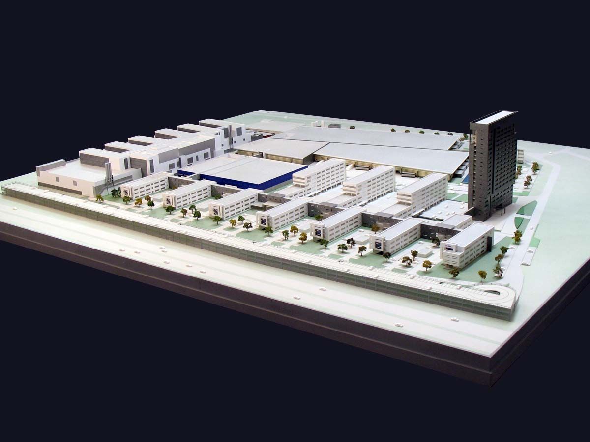
ASML, they make the machines that make machines—or, more precisely, the machines that make computer chips. Its location might be unassuming, but ASML holds an estimated 80-90%[1] market share in the global microchip market, counting giants such as Intel, Apple, TSMC, and others under their clientele. From the motorway alongside their headquarters, the only thing to indicate what it does is that the building itself resembles a monumental computer chip.

ASML was created after Dutch multinational conglomerate Philips bought out a small lithography company named ASMI – Advanced Semiconductor Materials International – in 1984. At the time, Philips was looking to split most Research & Development off from its main company, doing away with the mythical and historically well-funded Nat.Lab while retaining activities related to the development of nuclear power within its main holdings. Initially it housed its new venture – renamed ASML, replacing the aspirational ‘International’ in its name for the descriptive ‘Lithography’ – in a shed next to its headquarters in Eindhoven. In 1985, ASML moved to what is still today its headquarters in nearby Velthoven. Initially, the office buildings were designed to be modular: if the company were to fold, parts of its building could be rented out to others. Instead, the company has grown relentlessly over the past thirty years, and is now the Netherlands’ biggest in terms of both profit and value.
The relationship between Philips and ASML is a complicated one. Its licenced corporate history, The Money Machine: ASML’s Turbulent Youthby Renée Raaijmakers[2], identifies ASML as having been a struggling company, whose strong management culture of defiance towards its former parent company Philips made it a fertile environment for ‘wild innovation’. The book illustrates this history through the stories of the men involved in the inception of ASML, such as George de Kruiff—who puts his Philips job on the line to buy out the up-and-coming business ASMI—and the reserved Wim Troost—whose passion for computing drove Philips to buy the lithography business. When I visited ASML last summer, I spoke to an employee who gave me a different perspective. He said he ‘never expected to work for the same company all my career, and certainly not the one my dad worked for, too’. He had been at ASML for over 30 years, and his father had worked at the Philips factory for 40 years before him. If distance from Philips shaped ASML’s early corporate trajectory, the proximity to Philips is certainly felt on the factory floor.
The technology that manufactures microchips is called photolithography. It is a combination of photography—because it uses the principles of dark room printing—and lithography—as it uses techniques of stone etching into silicon wafers. A form of printing invented by German playwright Alois Senefelder in 1798, early lithography used stone from the Solnhofen limestone plateau to cheaply print sheet music and precise maps. Lithography has a longer history in this part of south Netherlands. Some five kilometers from Velthoven, in Valkenswaard, Peter-Louis Vrijdag inherited a lithographic printing plant for packaging materials from his grandfather. The collection of historical lithographic material that he built up over the course of his life serves as the foundation of the local lithography museum, founded in 2011. The latest addition to their collection is a PAS2500/10, a very early model of an ASML (then ASMI) photolithography machine from 1986.

Inside ASML’s newest photolithography machines, thousands of microchips are printed each minute on ‘wafers’: thin, circular slices of crystalline silicon, a semiconducting material. A ‘mask’ holds the blueprint for a wafer full of microchips in place. ASML machines focus light in the shape of these blueprints, which are are "designed" by clients of ASML such as Intel or TSMC, onto the silicon wafer in quick succession. Light sensitive coating material called ‘photoresist’ is etched away from the silicone surface, revealing the transistors that now form the basic architecture of computer chips. Each microchip contains millions of transistors, and each wafer contains a few thousand of individual chips. The process of focusing the light onto the wafer is repeated to form different layers vertically, of more than 40 layers of transistors stacked on top of each other.[3]
Transistors are the switches that enable the flow of electrons through a microchip. As semiconductor devices, they are made up of three components, one input, and two outputs; a capacitator, a resistor, and an inductor. This architecture is what makes computing digital, and binary. Early transistors were modelled on the hand:the three rods sticking out from a connecting component appeared like fingers, or digits. Its shrinking size was often modelled using the scale of a hand in advertisements, where transistors disappeared from the desk space, to the palm of the hand, onto the fingertip. The binary nature of transistor-based computing refers to transistors’ discrete outputs – neutral, on, or off. This is the basis of translating computer processing into text for human operators, expressed in strings of zeroes and ones.
The massive expansion of computing power from 1959 onwards—when the integrated circuit was first invented, an early name for what would later be known as a computer chip —has been made possible by the colossal compression of transistors on chips. This development has followed a line of growth prophesised by Gordon Moore in 1964, in an article named ‘Cramming More Components onto Integrated Circuits’. Its main thesis stems from the observation that since the invention of the integrated circuit five years previous, the amount of transistors that can be fit onto a single circuit has increased twofold annually. Only dubbed a ‘law’ years later by professor Carver Mead, Moore revised the law in 1974 to a twofold increase every 18 months. The number of transistors per chip has doubled at this rate ever since. As Moore’s law is exponential,each computer chip made now holds a few billion transistors each.
In its over 30 years of production, ASML has considered Moore’s law as a goal, and has worked to enhance the precision and speed of its machines to shrink transistor sizes down to atomic levels in order to keep up. In 2014, Moore admitted as much himself: ‘rather than becoming something that chronicled progress of the industry, Moore’s law became something that drove the industry…A tremendous amount of engineering and commitment has been required to make that happen.’[4] And in a 2015 interview with the Financial Times, ASML CEO Peter Wennink conceded that ‘our competition is not so much another company, it is Moore’s Law’.[5] If Moore’s law was devised as an unfolding potential, ASML has imbued itsprophecy with an enormous amount of agency, through which it pushes Moore’s law onwards and keeps it artificially alive.
Fulfilling the prophecy of Moore’s law has material repercussions. In his original proposal, Moore noted that the biggest challenge ahead would be heat, generated by the dense cramming of components onto a single chip. Transistors get hot through electrons, which operate at a subatomic level. Electrons carry charge, which is responsible for the creation of information. As electrons flow through a circuit, they generate heat when they encounter other particles. Most of the battery life of devices that feature integrated circuits today, like laptops and smartphones, is spent warming itself up. In order to prevent overheating, the increase of clock rates - the speed microchips perform calculations at, which is driven by the speed of electrons moving through the circuit - halted in 2004. Chips have continued to gain processing power since then, but they have ceased to match a once corresponding increase in speed.

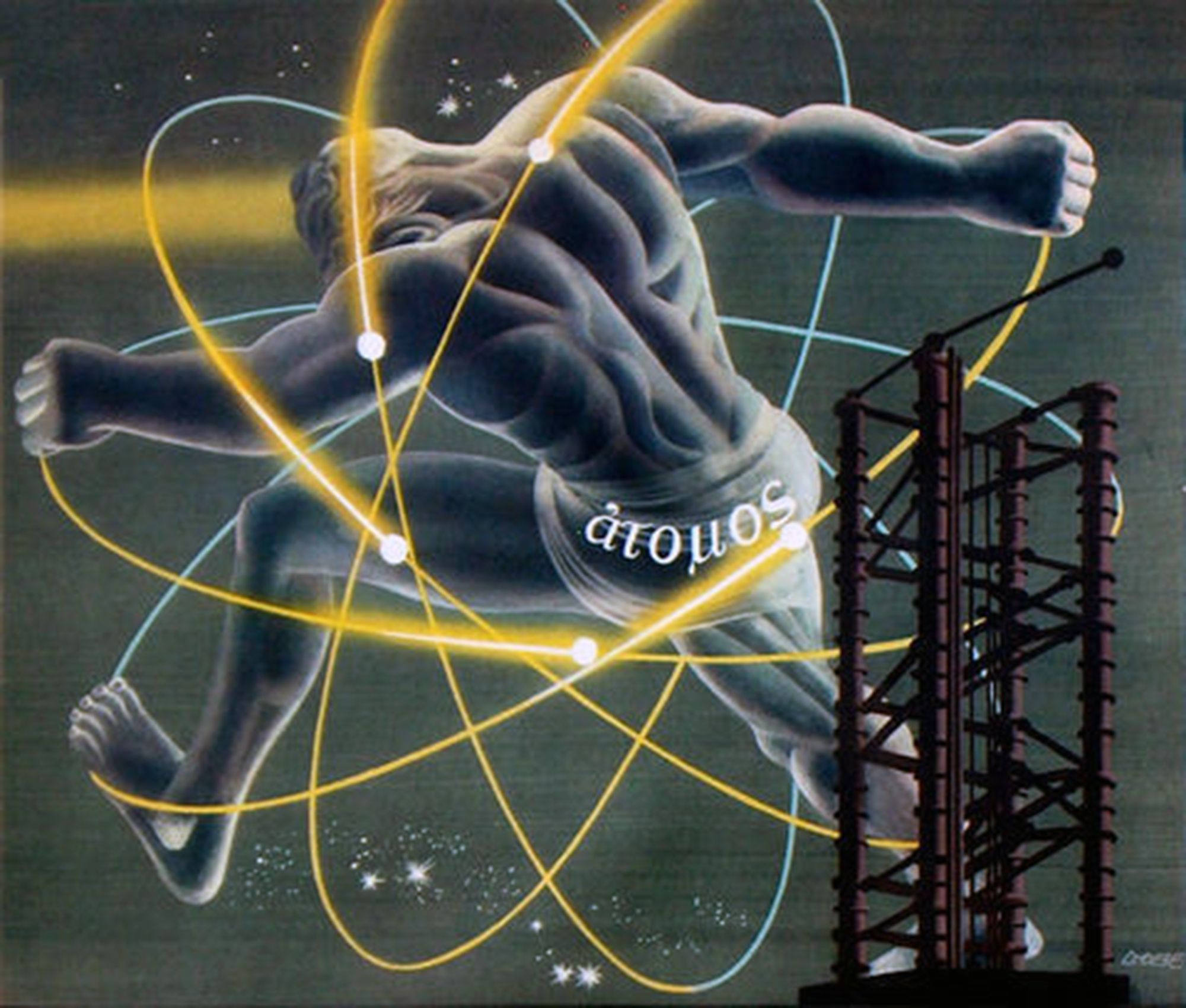
To continue increasing processing power while maintain clock rates, ASML shrunk transistors made on their machines down beyond a 22 nanometer resolution. To do this, they changed the very method by which they exposed light onto wafers. In 2007, ASML started developing extreme-ultraviolet (EUV) technology, first shipped in 2013. Doing away with reticules and lenses in favour of mirrors and more powerful lasers allowed ASML to lower the ‘benchmarks for transistor density’ to 8 nanometers, and continue to ‘[drive] Moore’s Law forward’[6]. This technology is heavily reliant on ultrapure tin, which is sprayed into the machine and exploded by lasers to into plasma at a rate of 50,000 times per second. In many of their promotional materials for EUV, the human scale is replaced by imagery that calls to mind the exponential energy of atomic explosions.

Keeping up with Moore’s law, packaging transistors tighter on a single plane leads to another issue: ‘electron bleed.’ With less space for electrons to travel in the circuit, the number of electrons that ‘jump’ from one place to another in the circuit increases, which heightens chip temperatures exponentially. Instead of packing transistors tighter alongside each other, chip manufacturers therefore stack layers of transistors on top of each other, more and more with each production cycle. Stacking layers of transistors consequently leads to another problem: the wafer bends upwards or downwards. This is dubbed the ‘sombrero’ or the ‘Marylin Monroe’ effect by ASML scientists, respectively referring to the rim of a Mexican hat or the iconic blowing upwards of a skirt. This leads to higher defects of chips per unit. Wafers are crammed to the rim; they’re bulging with escaping electrons. ASML outsources this issue to their clients to solve, as they are the ones making the blueprints. From their perspective, this maintains Moore’s law; the 18-month doubling persists.
Imaginaries of technological progress have been vastly saturated by computer chips since the invention of the integrated circuit in 1959. Since then, transistor sizes keep chipping away. The company that holds almost a 90% market share in this field remains dead set on fulfilling a prophecy that is 60 years old to drive its mission forward, and keep its profits soaring. In ASML’s advertisements, their machines are shown to crowd the size of the wafers, a standardised 300-mm slice, with ever more microchips. Their clients, in turn, advertise new technologies to consumers by stressing how their hardware contains more megapixels, more memory, more speed and more battery while maintinging or shrinking in size. As such, Moore’s law has overrun the imagination of what technological progress can look like. At the moment, the imagination that’s getting delivered is this: more powerful chips that maintain the same speed and keep getting hotter, produced by companies that are increasingly proprietary about the repairs of their wares and the public’s understanding of their inner workings. If there were a tarot card that ASML would draw about its future, it would be the Wheel of Fortune. At first read, the spinning wafers that feature those tiny slivers of silicone have delivered ASML its business fortune. But there is a Sisyphean perspective to this too: Moore’s Law is the destiny and the fortune of the company, the wheels that are spinning up the graphs in 18 month increments, evolving its technologies to end up in the same cycle 18 months per turn. Whether Moore’s Law will end, and if the end of Moore’s Law can explode our linear notion of technological progress, is a question the 21st century hasn’t seen the end of yet.
Footnotes
1. The Financial Times and Fitch Credit Ratings evaluate it to be 85 and 90 respectively. The discrepancy in these numbers is most likely caused by a confusion of ASML’s activities. Its business can be divided into two activities: systems and applications. Systems refers to the production of photolithography machines, where it is safe to say that more than 95% of the worlds’ chips are made on ASML machines; in terms of applications, they face some competition from Silicon Valley-based companies with large patent portfolios.
2. published on the occasion of ASML’s 30-year anniversary in 2017 in Dutch as De geldmachine - De turbulente jeugd van ASML.
3. ASMLCompany, 2014, ‘Our Stories – Gordon Moore About Moore’s Law’, YouTube, [online video], (18 December 2014).
4. Ibid.
5. Hook, L., 2015, ‘Peter Wennink, ASML: the memory maker: ’, Financial Times, [online]. (13th December 2015)
